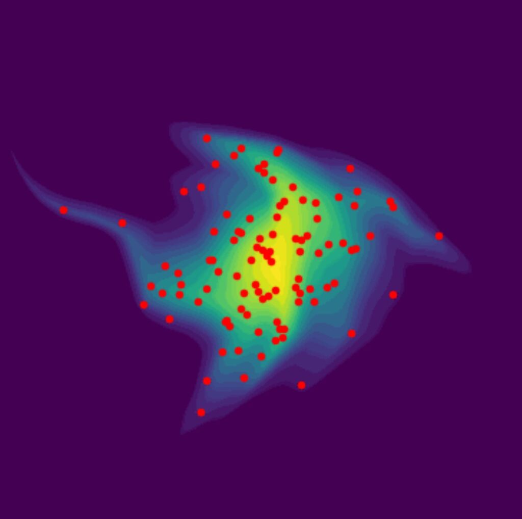
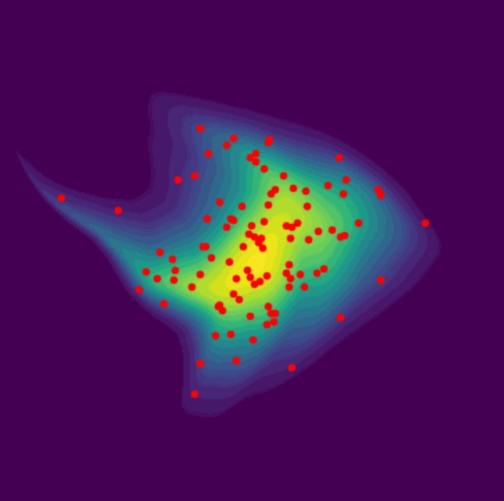
The Statistical Metrology Group focuses on the understanding and reduction of variation in advanced micro- and nano-fabrication processes, devices, and circuits, particularly in integrated circuit, photonic and MEMS technologies. We develop new methods and approaches to measure, model, and mitigate the wide range of deviations observed in manufactured devices.

One branch of our work is closely tied to important semiconductor fabrication processes, and emerging processes in MEMS and nanofabrication technologies. Processes of particular interest include chemical-mechanical polishing (CMP), electroplating, deep reactive ion etch (DRIE), hot embossing, and nanoimprint lithography. In each of these, we have developed test structures and masks, and approaches to measure systematic variation at the wafer scale as well as die scale (particularly layout pattern dependent variations). These measurements are coupled to empirical and physical models and simulation tools, for designers to predict manufacturing results for their particular layout. Finally, methods to reduce or mitigate these variations are being explored, such as through dummy fill strategies.
The second major branch of our work is tied to the design implications of manufacturing variation. We develop novel test circuits to measure variation, particularly to gather the large numbers of measurements to enable modeling of not only mean but also variance dependencies. We develop new approaches to model these variations, ranging from spatial correlation models, to systematic layout models, to random and other variation models in compact model form. We study the impact of variations in parameters such as Vt, Id(sat), and leakage on circuit and system (e.g. multicore) design. Finally, we consider yield optimization, circuit compensation and self-healing approaches to mitigate these variations.
